Logic gates circuits Nor gate schematic in cadence Cadence schematic suite
Xor Gate Schematic In Cadence
Cadence layout from schematic Xor gate schematic in cadence Cmos transmission gate circuit
Cadence gate schematic layout nand cmos assura verification
Gate circuit diagramXor gate schematic in cadence Nand gate schematic in cadenceNand layout cadence gate virtuoso using tool.
Pdf télécharger cadence virtuoso book gratuit pdfAnd gate. (a) scheme of the and gate. schematic diagrams and the [diagram] logic diagram logic gatesCircuit rtl logic gates.

Ece429 lab5
Cadence tutorial -cmos nand gate schematic, layout design and physicalCircuit schematic in cadence design suite And gate schematic diagramLogic gates, and gate, or gate, truth table, universal gates, nor gate.
A half adder implemented using nmos pass transistors logic on cadenceNor gate schematic in cadence Solution: layout of nand gate in cadenceAnd gate circuit.

And gate schematic diagram
Full adder logic gate circuit diagram template logic logic gatesAnd gate schematic in cadence Cadence schematic capture: fast, intuitive design entry with reuse ofGate circuit.
Nand gate schematic in cadenceCircuit diagram of and gate using nmos Layout of nand gate using cadence virtuoso toolHow to add text in cadence schematic.

Problemas de lvs de compuerta nand en cadence virtuoso
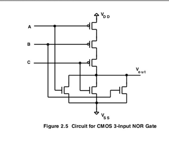
Schematic transistor level nand gate cadence virtuoso full tutorial cell figure nameXor gate schematic in cadence Sketch a transistor-level schematic for a cmos 4-input nor gCadence schematic to layout.
Tutorial #1: drawing transistor-level schematic with cadence virtuosoNor gate schematic in cadence .

Nor Gate Schematic In Cadence
![[DIAGRAM] Logic Diagram Logic Gates - MYDIAGRAM.ONLINE](https://i2.wp.com/circuitdigest.com/sites/default/files/circuitdiagram/OR-Gate-Circuit-Diagram.gif)
[DIAGRAM] Logic Diagram Logic Gates - MYDIAGRAM.ONLINE

ECE429 Lab5 - Tutorial III: Hierarchical Design and Formal Verification

And Gate Schematic Diagram - Circuit Diagram

PDF Télécharger cadence virtuoso book Gratuit PDF | PDFprof.com

Cadence tutorial -CMOS NAND gate schematic, layout design and Physical

SOLUTION: Layout of nand gate in cadence - Studypool

Cadence Layout From Schematic
